
An Fpga Integrated Circuit is a programmable digital device that can change its hardware behavior after manufacturing. Unlike a fixed-function chip, it contains configurable logic blocks, flip-flops, memory, and programmable routing. Engineers connect these elements through a configuration bitstream. The result can resemble a processor, signal filter, communication controller, or specialized accelerator.
Ross Freeman, Xilinx co-founder and FPGA co-inventor, described this flexibility clearly: “The FPGA is a blank slate.” His words remain useful because they explain the device’s central value. The chip does not begin as a finished circuit. Instead, design software maps logical operations into physical resources inside the silicon. A clock signal may move through carefully selected paths, while lookup tables perform calculations and registers hold changing data. Small details matter. Routing delays, clock skew, power use, and available logic can decide whether a design works reliably.
However, a simple explanation can become misleading. An FPGA is not automatically faster than every processor or ASIC. It often needs careful timing analysis, hardware description languages, simulation, and repeated testing. The development process may feel less direct than writing software. Still, its reconfigurability makes it valuable when requirements may change. A factory controller, radar interface, or medical imaging prototype can receive new logic without replacing the entire board. That advantage has limits. Configuration errors can produce unexpected behavior, and poor architecture can waste valuable resources. This guide examines the internal structure of an Fpga Integrated Circuit, follows its configuration process, and explains where its practical strengths—and weaknesses—appear in real engineering work.
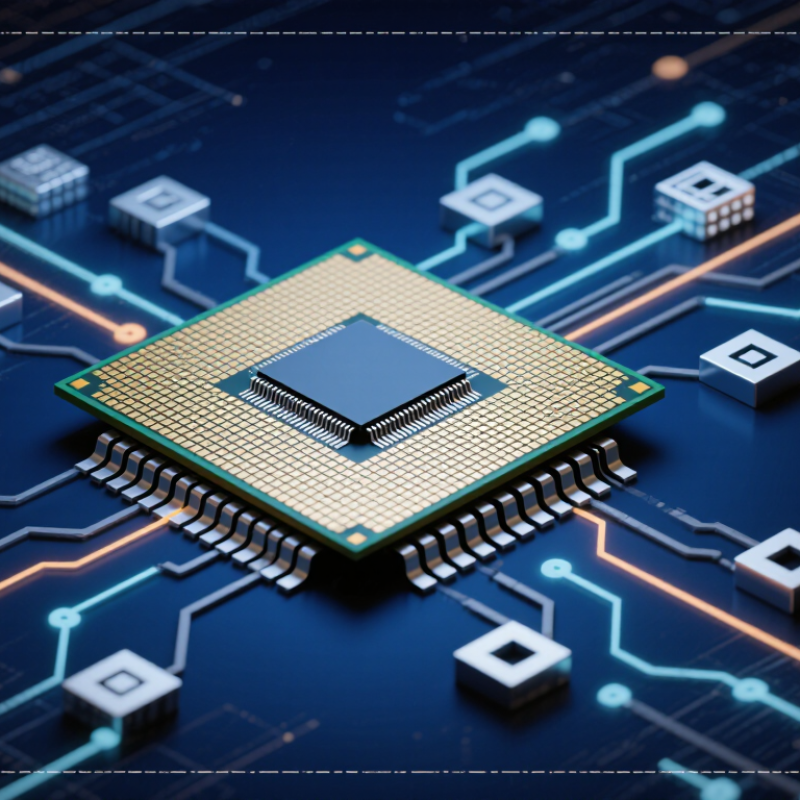
An FPGA integrated circuit is a reconfigurable hardware device. Its architecture lets engineers build digital functions after manufacturing. Unlike a fixed circuit, it can be programmed repeatedly for control, signal processing, or rapid prototypes.
At the center are logic cells built from 6-input lookup tables, or LUTs. A LUT stores truth-table values and produces one output for many input combinations. Some LUTs can split into smaller functions, improving resource use. Flip-flops sit beside the LUTs and preserve bits on clock edges. They create registers, counters, pipelines, and state machines. Programmable routing then connects these blocks through switch matrices. This network is powerful, but long routes add delay and may weaken timing performance. In high-end devices, the fabric can exceed 10 million logic cells, although vendors define “logic cell” differently. That detail deserves careful checking.
Tips:
Keep related signals physically close. Use pipeline stages when a path becomes too slow. Check the timing report, not only the simulation.
In practical development, I often treat routing as a design resource, not an afterthought. A small arithmetic block may work perfectly in simulation, yet fail its target clock after placement. The lesson is uncomfortable: more logic capacity does not guarantee better speed. Designers must balance LUT usage, flip-flop placement, routing congestion, clock structure, and power. I still review these trade-offs repeatedly, because an apparently elegant architecture can become inefficient after implementation.
An FPGA is a programmable integrated circuit built from logic blocks, routing channels, and configurable input/output circuits. Its behavior is not permanently fixed during manufacture. Instead, configuration memory stores a digital file called a bitstream. This file describes how each logic block and routing switch should behave.
Most FPGAs use SRAM cells for configuration storage. SRAM is fast and flexible, but it is volatile. The data disappears when power is removed. During startup, a controller receives the bitstream from an external memory device or another system. It shifts configuration data into the FPGA through a defined interface. The stream is usually divided into frames, which update specific regions of the device. Tiny memory cells then control lookup-table contents, signal multiplexers, routing switches, and timing options.
The process resembles setting thousands of microscopic switches before operation begins. A valid bitstream can connect a counter to an output pin, while another can create a signal-processing pipeline. Engineers often verify loading with status signals, configuration checks, and a clock observed on test equipment. Small errors matter. A damaged bitstream may leave the device partly configured, not simply “off.” This is where simplified explanations fail: SRAM does not execute instructions like a processor. It holds control states that reshape hardware connections. Designers must also consider startup time, data integrity, power interruption, and whether the configured circuit matches the intended hardware.
An FPGA integrated circuit contains configurable logic blocks, routing resources, memory elements, and input/output interfaces. Engineers describe intended behavior with HDL, often at register-transfer level, before hardware resources are assigned. A clocked counter, packet filter, or control state machine becomes synthesizable logic. The result is not software running on a processor. It is a programmed electrical structure.
During synthesis, tools parse HDL, infer registers, simplify Boolean expressions, and map functions into available primitives. Poorly written loops or incomplete assignments can create unintended storage or excessive logic. I have found that readable RTL usually makes timing problems easier to trace, although readability alone cannot guarantee efficiency. Constraints then define clock periods, input delays, output delays, and relationships between clock domains. Missing constraints are dangerous.
Placement assigns each logical element a physical location on the chip. Routing connects those locations through programmable wires and switches, while timing analysis measures delay across every critical path. If a data path misses its deadline, engineers may pipeline it, reduce fanout, restructure arithmetic, or adjust placement guidance. Timing closure is iterative, not ceremonial. A design can pass synthesis and still fail after routing because wire delay dominates a crowded region. Reviewing reports, checking clock-domain crossings, and testing reset behavior provide evidence beyond a clean compilation. One practical weakness remains: estimates change as the design grows. Measure early.
An FPGA integrated circuit is a configurable logic device that turns a hardware description into a working digital system. Its strength becomes clear when one task can be divided into many operations. Instead of processing every sample in sequence, the circuit can run hundreds of hardware pipelines at the same time. Each pipeline may filter data, detect edges, or calculate a control value.
DSP blocks handle repeated mathematical work, such as multiplication, addition, and finite impulse response filtering. Their fixed structure usually delivers better speed and power efficiency than building every operation from general logic. BRAM provides fast local storage for coefficients, line buffers, lookup tables, and temporary results. Data can move between pipelines without waiting for a distant memory system.
A video stream makes the idea concrete. One pipeline reads pixels, another removes noise, and a third calculates motion features. All three can remain active on different pixels during the same clock cycle. Timing still matters. A design may contain enough logic but fail because signals arrive too late. That assumption is easy to miss.
In practice, engineers inspect latency, memory bandwidth, clock constraints, and numerical precision together. Wider numbers improve accuracy but consume more resources. Smaller numbers save space but may create visible errors. The best architecture is rarely perfect; it is a careful compromise tested with real input data, not only simulated examples.
An FPGA integrated circuit contains programmable logic blocks, routing channels, memory, and clock networks. Unlike fixed-function silicon, it can be configured after manufacturing. Engineers build data paths by connecting logic cells through internal routing. The practical advantage is flexibility. A design can process sensor data, packets, or control signals without changing the circuit board. But programmable does not mean effortless.
With carefully constrained designs, FPGA logic can exceed 500 MHz. That speed represents a two-nanosecond clock period. Every register, route, and clock transition must fit inside it. Designers use deep pipelining, balanced clocks, and placement constraints to protect timing margins. One long routing path can break an otherwise correct design. Simulation may pass. Hardware can still fail.
High-speed transceivers support serial links above 28 Gb/s per lane. They convert parallel logic into carefully timed electrical symbols, then recover the data at the receiver. At this rate, connector quality, trace length, impedance, and signal loss become critical. Engineers inspect eye diagrams, measure bit-error rates, and test across voltage and temperature changes. Small mistakes become visible quickly. A reliable interface also needs buffering, lane alignment, clock recovery, and error monitoring. The difficult part is not reaching a headline speed; it is maintaining stable performance under real operating conditions.